
3.jpeg)
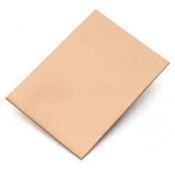
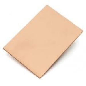
Copper Clad Laminate Double Side PCB – 100 x 75 x 1.5 mm
₹ 71
₹ 119


| : | |
| Made In : | India |
The Copper Clad Laminate Double Side PCB is a high-quality base board used for designing and developing custom electronic circuits. With copper coating on both sides, it allows efficient routing of complex circuits, making it ideal for prototyping, DIY electronics, and industrial PCB fabrication.
Its durable FR4 base ensures mechanical strength and excellent thermal stability, suitable for soldering and etching processes.
Key Features
- Double-sided copper coating for flexible circuit design
- High-quality FR4 fiberglass base material
- Standard size: 100 × 75 mm
- Thickness: 1.5 mm for durability
- Excellent conductivity and solderability
- Suitable for etching and drilling
- Heat resistant and mechanically strong
- Ideal for DIY and professional PCB fabrication
- Compatible with all electronic components mounting
Technical Specifications
| Parameter | Specification |
|---|---|
| Material | FR4 Fiberglass with Copper Lamination |
| Board Type | Double Side Copper Clad PCB |
| Dimensions | 100 × 75 mm |
| Thickness | 1.5 mm |
| Copper Layer | Dual-sided (Top & Bottom) |
| Copper Thickness | ~35 µm (standard) |
| Thermal Resistance | High |
| Electrical Insulation | Excellent between layers |
| Surface Finish | Plain copper (unetched) |
How to Use
- Design circuit layout using PCB design software
- Transfer pattern using toner transfer or UV method
- Etch unwanted copper using ferric chloride solution
- Drill holes for component placement
- Solder electronic components on copper tracks
- Use both sides for complex circuit routing
- Clean and inspect before powering circuit
Applications
- DIY electronics projects
- Arduino and ESP32 circuit prototyping
- Robotics control boards
- Power supply circuit design
- Embedded system development
- Educational electronics training
- Industrial PCB prototyping
- Sensor and IoT circuit development
Package Includes
1 * Copper Clad Laminate Double Side PCB – 100 x 75 x 1.5 mm
0 Reviews For this Product

Related Products